|
Our research on H:Si devices is primarily motivated by the need to develop high quality (mobility) electron systems in Si that are amenable to fabrication techniques at or near the atomic scale. The physics of electron systems in these devices is of interest in its own right: in particular the valley degeneracy of the electrons is dependent on surface orientation. We are studying [111] oriented surfaces (in which each Si surface bond is pointing perpendicular to the surface and is terminated by one H atom) for two reasons: the valley degeneracy is predicted to be the maximum possible value of six and because chemical treatments of Si [111] yield atomically smooth surfaces. |
|
A [111] oriented hydrogen terminated surface. In this orientation the hydrogen bonds are perpendicular to the surface. Atomically flat surfaces can be prepared in this orientation because some chemical etchants preferentially remove protruding silicon atoms and thus flatten the surface. For more information, please see our interactive model of a silicon [111] surface. |
Hydrogen-terminated Silicon Surface Devices |


|
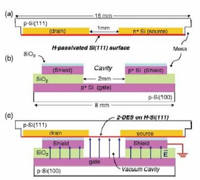
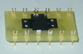
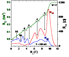
H:Si[111] surface electrons in bonded FET structures Because there is a very low density of surface states on H:Si surfaces, electrons can be induced on the surface by a strong electric field, and the induced electrons can be probed by transport measurements if ohmic contacts are present.. In our current devices contacts are created by ion implantation into a Si[111] chip, which is bonded to a silicon-on insulator (SOI) chip that contains a conducting gate and a vacuum cavity across which the electric field is applied. All of the processes necessary for fabrication are standard except for the chip scale bonding step, which requires that the two surfaces be extremely flat and clean so that they adhere to one another by van der Waals forces. Additionally, just prior to bonding, the Si[111] surface must be treated with NH4F in an oxygen-free environment. Once bonded together the chips are wired up using indium contacts and gold wire. At low temperatures the electron mobility can exceed 100,000 cm2/Vsec, much higher that what is achievable in MOS (metal-oxide-silicon) FETs. Our investigation of these types of devices has only just begun, and there are many possible future avenues of research. |
|
Silicon-based quantum computing home page B. E. Kane November,2010 |
