Electrical Characterization of Operating PN Junction with
Conductance Mapping and STM
High spatial resolution
characterization techniques capable of probing dopant profile, electrostatic potential
or carrier charge density, are needed as enabling technologies for the
continued increase in density and decrease of size of semiconductor
devices. The highest resolution probe
available is scanning tunneling microscopy (STM), which we have previously [1]
used to delineate a depletion zone related feature within a Si pn
junction. The coupling of
topographical and electronic information in STM measurements complicates
interpretation of the images.
Recently, we have implemented the instrumentation necessary for
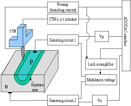
Fig. 1. Schematic of instrumentation for
conductance/topography mapping.
simultaneous measurement of
topography and conductance, using an STM.
Our measured conductance maps from oxide-terminated pn junctions allow
delineation of different regions within the junction [2]. The interpretation of these maps is that
large conductance corresponds to a tip-gap -semiconductor junction electrically
in either accumulation or strong inversion, and smaller conductance to a
junction in weak inversion or depletion.
This in turn identifies the type and concentration of majority charge
carriers in the area probed by the STM tip.
Maps acquired while ramping of the applied pn-junction bias confirm our
earlier interpretation of the electronic nature of “dips” in the STM images
[1], i.e. that they are regions of inverted carrier charge: hole dominated in
spite of the n-type doping due to their location within the depletion zone.
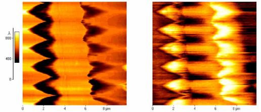
Fig. 2. Topography map (left) and conductance map (right) of oxide
covered Si device consisting
of p+ “stripe” within n-type Si substrate, acquired while ramping
the pn reverse bias back and
forth from 0 to 10 volts. p+ stripe is the broad region right of
center. Depletion zone features
are the wedge-shaped regions.
[1] M. L. Hildner, R. J. Phaneuf and E. D. Williams, Appl. Phys. Lett. 72, 3314 (1998).
[2] J. Y. Park, R. J. Phaneuf and E. D. Williams, submitted to J. Appl. Phys. (2001)