In recent years a number of microscopies originally developed for surface studies have been applied to the characterization of semiconductor device structures. Surface/interface effects can provide contrast according to spatial variations in doping, carrier charge density and/or electrostatic potential, however they also complicate the analysis of the images. For example, for a semiconductor the existence of a large density of surface-states or terminating oxide interface-states within the bulk-forbidden energy gap can result in the formation of a space charge layer and a variation in the electron energy levels with depth beneath the semiconductor surface, or “band-bending”. There also exists a lateral band-bending or “band line up” across the device (within the surface/interface plane)
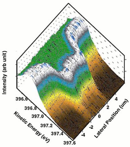
Fig. 1. Composite “Image” of lateral band bending across the two pn junctions
separating a heavily doped (1E18/cm^3) p-type stripe from the surrounding lightly
n-doped (1.6E14/cm^3) Si substrate. Assembled from 16 individual SPEM
intensity maps (including those of Fig. 4) whose energies bound the unreacted
Si 2p 3/2 core level (ridge of intensity in this image).
associated with lateral variations in space charge. The importance of these effects for device performance makes it desirable to record spectroscopically-resolved images, so that the variation in the energy levels across a device can be “imaged” directly. We have shown that near-threshold photoelectron emission microscopy (PEEM) images of Si pn junctions show contrast according to doping which we interpreted as due to a variation of the near-surface band-bending with doping [1,2]. The lack of an electron energy analyzer, however prevented a direct quantitative measurement of this effect. More recently we used scanning photoelectron microscopy (SPEM) developed at the
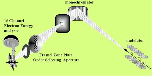
Fig. 2. Schematic of beamline
and scanning xray photoemission microscope at
Elettra used in these
experiments.
Elettra synchrotron light source in Trieste to characterize the same lateral Si pn-junction arrays imaged previously with PEEM and STM [3]. With the SPEM we measured both energetically-resolved images (see Fig. 4) of the surface of the devices and spatially-resolved spectra (see Fig. 3). Our results show that the energy
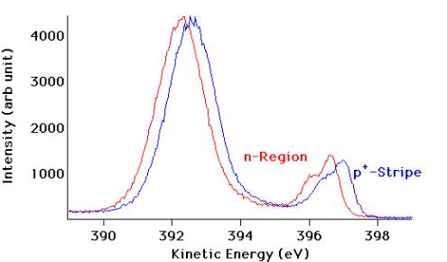
Fig. 3. Si 2p core level spectra acquired from within n-type region
(red) and
p-type (blue) region of
pn-array, measured through a 11 angstrom thick wet
chemical oxide..
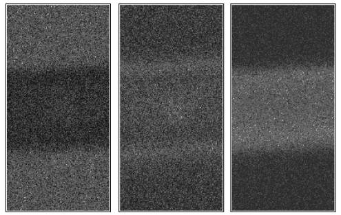
Fig. 4. Si 2p Intensity maps showing energy dependent contrast across one
p-stripe (center
of each map) of array and surrounding n-type Si substrate
acquired at an
xray energy of 496.4 eV and electron kinetic energies of
396.82 eV, 396.98
eV, and 397.22 eV (left-to right).
bands bend across the space charge region by an amount which varies with oxide preparation. We also are able to identify features in the images and spectra, which are clearly due to anomalous spatial variations in show that the energy bands bend across the space charge region by an amount which varies with oxide preparation. We are also able to identify features in the images and spectra which are clearly due to anomalous variations in the doping profile across the pn-junction. To our knowledge, this is the first time a pn-junction has been imaged with sufficient energy and spatial resolution to allow the transition-region band bending to be resolved and studied in detail.
![]()
[1] M. Giesen, R. J. Phaneuf, E. D. Williams, T. L. Einstein and H. Ibach, Appl. Phys. A 64, 423 (1997).
[2] V. Ballarotto, K. Siegrist, R. J. Phaneuf and E. D. Williams, Surf. Sci. 461 L570 (2000).
[3] R. J. Phaneuf, H. C. Kan, M. Marsi, L. Gregoratti, S. Gunther and L. Gregoratti, J. Appl. Phys. 88, 863 (2000).