Low Energy Electron Microscopy: Imaging Surface
Dynamics
Flexibility and time resolution make LEEM a powerful tool for studying mesoscale phenomena - from surface diffusion to
magnetization.
Raymond J. Phaneuf and
Andreas K. Schmid*
Physics
Today, vol. 56, no. 3, March 2003
In 1985 a stunning set of images was published by Ernst Bauer and his student Wolfgang Telieps which abruptly solved a long-debated question in surface science, the nature of the phase transition which occurs on the (111) surface of silicon [1]. One of their images shown as Fig. 1 shows that there is a sharply defined coexistence between two structural phases, demonstrating a first order - rather than a continuous transition - between ordered (bright) and disordered (dark) arrangement of atoms at the surface. Determination of the complex ordered arrangement of atoms, or “reconstruction” that occurs on the Si(111) surface beneath approximately 860°C had been one of the hottest problems in surface science for
nearly 25 years, and had just been
solved [2]. Bauer and Telieps’ unambiguous answer about the nature of its
disordering transition was a dramatic introduction of a very powerful probe of
solid surfaces, low energy electron microscopy (LEEM).
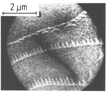
![Text Box: Figure 1. Coexisting phases on the (111) surface of silicon. The contrast between light and dark regions illustrates the sharp division between the phases. Bright regions are ordered, with a unit cell seven times as large as the bulk Si spacing in each of two high symmetry directions-referred to as (7x7) reconstructed-and darker regions contain a disordered lattice gas of Si atoms. That surface disordered structure is referred to as a “(1x1)” phase, because of periodicity below the top layer. The dark diagonal line is a crack in the detector. (Adapted from reference [1]).](LEEM_PhysicsToday_files/image014.gif)
Since publication of those early images an increasing number of investigators have used LEEM to gain insights into a variety of dynamical processes on surfaces. After all, whether the interest is crystal growth, thin-film or multilayer materials engineering, or catalysis, the importance of surface science is based on understanding surfaces not as static objects, but as dynamic systems. Key questions include, for example: how do structural transitions nucleate and propagate across a surface? What are the limiting processes in atom transport across a surface during temperature treatments or material deposition?
At roughly the same time that successful LEEM research began, atomic resolution capability made scanning tunneling microscopy an important technique in surface science, allowing the determination of the arrangements of atoms within many of the ordered reconstructions and disordered structures which occur at surfaces. While the lateral resolution of LEEM is more limited, the advantages of inherently high imaging rate, large field of view, and easily variable sample environment have made LEEM the technique of choice for studying many of the outstanding problems regarding the dynamic properties of surfaces. .
LEEM and its variations combine a number of spectroscopic techniques and use the fact- already exploited in low energy electron diffraction – that electrons with energies of a few to a few tens of eV are extremely sensitive to near-surface atomic order. Depending on the energy of the incident electron beam, subtle differences in local atomic structure or composition can give rise to dramatic contrast in LEEM images. An example is the contrast, evident in figure 1, which results from a strong difference in specularly diffracted intensity between the ordered and disordered structures. What distinguishes LEEM from LEED and other scattering techniques is its real-time surface imaging capability (although the diffraction pattern is still available in the back focal plane of the objective lens). Image formation with electrons is analogous to light-microscope imaging; the backscattered electron beam diverges and refocuses through electrostatic or magnetic lenses on its way to a phosphor screen (see the box on page XX). LEEM is the fruit of more than 20 years of work by Bauer, who recognized by the early 1960’s that the high reflectivity of electrons from surfaces at low energies would make surface sensitive imaging practical. The first published images caused great excitement in the surface science community, demonstrating that the LEEM allowed images of surfaces to be acquired with high spatial resolution, typically several nm, and at video rates. One may image in-situ samples over a wide range of temperatures and in the presence of incident fluxes of atoms, ions or light. That flexibility, for example, allows researchers to more easily control the evolution of nanostructures.
Cobalt on silicon
Bauer and Telieps’ initial
observation of phase coexistence became the starting point for a growing number
of discoveries using LEEM. One crucial problem in modifying surfaces is how the
deposition of atoms of a different element modifies the structures that form
and coexist. For example, one of us
(Phaneuf) and Peter Bennett at
That insight about the transition would be almost impossible from diffraction studies alone, as the disordered structure produces no extra reflections in the diffraction pattern. Increasing the Co coverage produces a large and continuous change of the transition temperature, with a depression of 170°C resulting from only a tenth of a monolayer. The driving force for this is well known from bulk alloy systems: Adding an insoluble impurity to a solid phase results in a lowering of its melting point to allow the segregation of the impurity to the liquid phase where its solubility is higher. In our case lowering the disordering temperature allows Co-containing clusters to segregate out of the ordered surface regions into the disordered phase. The shape of the phase boundary in Fig. 2(c) indicates the presence of a small repulsion between the Co-containing particles in the disordered phase.
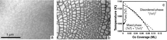
![Text Box: Figure 2. Cobalt on Si(111). (a) The clean Si surface was confirmed to be an ordered (7x7) reconstruction from its diffraction pattern. (b) After 0.02 monolayer had been adsorbed, the dark regions appeared. They were a disordered lattice-gas of Co-containing clusters that segregated to steps (the longer lines) and domain boundaries (the shorter lines). (c) A clear phase boundary separates a region of coexistence from a pure disordered phase. Solid dots indicate the temperatures at which the surface disorders on heating and open squares indicate the temperatures at which the phase coexistence appears on cooling. The solid curve shows a fit to the Clapyeron equation including a repulsive interaction between Co-containing clusters in the disordered phase. The dashed straight line is for the noninteracting case (Adapted from reference [3]).](LEEM_PhysicsToday_files/image019.gif)
Even for atomically clean Si(111) surfaces, the fact that there are coexisting ordered and disordered regions at all is surprising. At first sight, this seems to be at odds with the Gibbs phase rule which predicts that only a single phase should exist at a given temperature and pressure, and that there should be sharp transitions between phases. Using their LEEM, Jim Hannon and his collaborators at IBM [5] recently discovered that long-range interactions between phase boundaries preclude a sharp transition between phases, even when the defect free regions of the surface are arbitrarily large, the so-called “thermodynamic limit”. The nature of the domain boundary interactions can stem from the two phases having different surface stresses or from their having different work functions. The temperature dependence of the relative sizes of the two types of regions on the surface is consistent with a model that includes a term in the free energy corresponding to the elastic interaction between “force monopoles” at the boundaries between phases.
Step Dynamics
The use of LEEM has progressed gradually, from qualitative analysis of images to fully quantitative analysis. The almost unique ability of the LEEM to form real-time surface sensitive images over a wide range of temperatures and conditions has now been used by a number of investigators to extract thermodynamic quantities which would be difficult, if not impossible to obtain by other techniques.
Consider the work of Ruud Tromp and his collaborators at IBM [6]. Those researchers observed Brownian motions of monolayer height surface steps and studied the evolution of monolayer height islands on the (001) surface of Si. Both phenomena are mediated by the attachment and detachment of Si atoms from the edges of the steps or islands, and their diffusion across the surface. Which of the activated atomic mechanisms is rate limiting, attachment/detachment or diffusion? Thermodynamics distinguishes the two cases based on a statistical analysis of the Fourier components of the spatial and temporal correlations along a fluctuating step edge. In particular one prediction is that the amplitude of the Fourier component corresponding to the wavevector q=2p/l, A(q) should be inversely proportional to l2 if attachment/detachment is rate limiting, but to l 3 if instead fluctuations result from a diffusion-limited process. (see discussions in the articles by Zoltan Torozckai and Ellen Williams, Physics Today, December 1999, p. 24 and by Harold Zandvliet, Bene Poelsma and Brian Swartzentruber, Physics Today, July 2001, p. 40.)
In an impressively detailed analysis, Norm Bartelt used a total of more than 35x106 step edge positions from image sequences acquired over the range of temperatures from 640°C to 1210°C [6]. He convincingly demonstrated a linear dependence of the inverse amplitude on l 2 in agreement with the prediction of attachment/detachment limited kinetics. Remarkably, those observations confirmed that that the conventional picture of surfaces as static is not at all correct. Instead, huge numbers of atoms move back and forth across the surface on a time scale of seconds. It also turns out that two different types of steps can be distinguished on the Si(001) surface; the origin of this difference is the relative orientation between a step and the anisotropic reconstruction; that reconstruction consists of rows atom-pairs that have shifted together to allow overlap dangling bonds. The two types of steps have different values of step free energy, or “stiffness”, leading to different fluctuation amplitudes observable in the LEEM data. Using the measured stiffness of both types of steps as a function of temperature, Bartelt determined precisely the fundamental energies which govern the motion of steps on the surface.
Island Ripening
Wolfgang Theis, Bartelt and Tromp [6] also studied the “ripening” which occurs at sufficiently high temperature, as larger islands grow at the expense of smaller islands on the surface. The well-known Gibbs-Thomson effect, in which the chemical potential of an island is proportional to the inverse of its radius of curvature, explains the ripening. Fig. 3(a) and (b) show LEEM snapshots of how a configuration of islands coexisting on the surface has evolved. One might have guessed that the time dependence of the sizes of islands on the surface could be predicted from a mean-field model in which a uniform chemical potential described the sea of atoms diffusing from island to island. As it turns out, this idea is nearly correct: Starting with a refined approximation – allowing the chemical potential in different cells around each island to take on different values, depending on island sizes - the model becomes essentially perfect. Compare the experimental measurement in figure 3(b) with the results from the computations in Fig 3(c). What’s striking is that the refined model successfully predicts not merely average island properties as a function of time. In fact, the model is sufficiently accurate to predict the histories of the individual islands, which the LEEM images allow to be followed in detail, as they ripen over time.
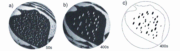
![Text Box: Figure 3. Atomistic diffusion on silicon-Small clusters are seen to grow into larger island in these 5.5 mm images. Atom high steps separate the alternating light and dark regions; the contrast results from a 90° rotation of the ordered-atom arrangement across the steps. (a) Small white elliptical clusters form after 0.1 Si monolayer is adsorbed at room temperature, and the temperature is raised for 50 s to 670°C. (b) the image 400 s later shows the effect of “ripening” in which larger islands appear to have swallowed smaller ones. (c) A numerical mean-field model , including different chemical potentials in cells around each island, evolved to this configuration, a nearly perfect prediction of the experimental progression (Adapted from reference [6].)](LEEM_PhysicsToday_files/image020.gif)
These observations highlight the importance of the sea of detached atoms, which is always present on surfaces at finite temperature. Though this “adatom lattice gas” is too dilute and too mobile to be observed directly, Tromp and Marian Mankos [6] successfully measured its density. They analyzed the appearance of islands on extremely large step-free regions of a lithographically altered Si(001) surface subsequent to an abrupt drop in temperature. Presumably, those islands were made up of atoms that were in the adatom lattice gas phase before the temperature was dropped. Measuring the sizes of these islands, the researchers were able to extract the concentration of Si atoms on the surface as a function of temperature. A simple Arrhenius model indicates that the diffusing species on the surface is not isolated atoms at all, but pairs of atoms, or “dimers”. These same dimers are known from STM images to line up in rows to form the anisotropic reconstruction mentioned above.
Self Assembly
Many of the early experiments - and those showcased in this article so far - concentrated on silicon surfaces because of Si’s technological importance, and the ease with which flat, atomically clean surfaces can be prepared. However a number of groups have investigated the evolution of metal surfaces during deposition, alloying or relaxation toward equilibrium. A striking example of the rich variety of phenomena that can occur as an alloy system orders comes from recent work by Gary Kellogg’s group at Sandia National Laboratories [7]. Using LEEM, those researchers observed self assembly on the nanometer length scale during the deposition of lead vapor onto the atomically clean (111) surface of copper at a temperature of 400°C [9]. Initially the deposition of Pb at this temperature results in the formation of a disordered Pb-Cu alloy. Once the alloy covers the surface, additional lead beads up into compact, nearly circular 70 nm islands. As the coverage increases the islands begin to order into a hexagonal pattern, that Richard Plass describes as a droplet phase (Fig. 4(a)). After still more coverage the islands coallesce into a configuration of stripes (Fig. 4(b)) and then into an arrangement of holes in the lead matrix or “negative droplet” phase (Fig. 4(c)).
Figure 4. Surface-alloy patterns of lead self assembling on copper(111). As
more lead adsorbs onto the surface, low-energy electron micrographs
indicate the formation of: (a) droplets (at 0.33 monolayer of Pb), (b)
stripes (0.38 monolayer), and (c) inverted droplets (0.48 monolayer).
Images were recorded using 18-eV energy electrons, with about 400 s
separating each picture. The Pb overlayer phase appears bright and the surface alloy
phase appears dark. (from reference [7]).
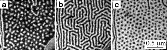

The still images, acquired over several minutes, do not convey the richness of the evolution of the structures’ evolution: the nucleation of droplets containing tens of thousands of atoms occurring in a single 30 ms frame. Observation of individual droplets reveals that the islands move within a force field corresponding to dipole-dipole interactions. That motion is consistent with the idea that the interaction forces between islands are mediated by strain fields generated within the substrate. It is remarkable, and perhaps unexpected, that this behavior depends on a high mobility of solid, crystalline islands containing hundreds of thousands of Pb atoms. The discovery of self-assembly on a mesoscopic length scale highlights the benefit of LEEM with its unique combination of high data rate and control of the sample environment.
Magnetic Phenomena
The examples discussed so far illustrate what sort of surface features - atomic surface steps and domains of different atomic structure, for instance - or composition are some of produce strong contrast using conventional LEEM sources. A spin-polarized electron source extends LEEM’s sensitivity to include magnetic phenomena. When a spin-polarized beam of low-energy electrons illuminates a magnetized surface, the reflectivity of the surface can vary dramatically depending on the relative orientation between the spin of the scattering electrons and the magnetization vector. Bauer’s group pioneered using this exchange scattering asymmetry for imaging, by developing the first spin-polarized LEEM or SPLEEM. In these microscopes, the orientation of the spin-polarization of the illuminating electron beam is adjustable. So, comparing a set of images that were recorded using different beam polarizations permits the determination of the local orientation of the magnetization vector in magnetic domains. Usually, one first uses opposite polarization alignments of the illumination beam to record two images with opposite magnetic contrast. Then, by forming a pixel-by-pixel difference image, magnetic contrast is enhanced, while simultaneously other LEEM contrast mechanisms are suppressed. Since the instrument records pairs of LEEM images, the SPLEEM technique is marginally slower than conventional LEEM, but shares the advantages of an easily variable sample environment.
In-situ sample processing is particularly interesting for magnetic materials, because magnetic properties depend very sensitively on microstructure. SPLEEM offers the capability to track the evolution of both structural- and magnetic properties simultaneously. For example, Thomas Duden summarized in his recent review [9] how magnetic thin films and multilayers can be grown in-situ, while simultaneously recording magnetic thin films and multilayers can be grown in situ while one simultaneously records LEEM images of the sample morphology and SPLEEM images of the exchange scattering asymmetry.
How magnetic microstructure responds to changing conditions of temperature or externally applied fields is an important questions both for applications and basic physics. Using a SPLEEM at Lawrence Berkeley Lab, Helmut Poppa and one of us (Schmid) recently demonstrated the feasibility of operating a SPLEEM while simultaneously applying a controllable magnetic field to the sample [10]. A particularly interesting case of field-dependent magnetic domain patterns occurs in thin film samples which have a magnetic anisotropy perpendicular to the film. Fig. 5 (a) shows a typical SPLEEM image of the zero-field domain structure of a 2.5 monolayer thick film of Fe on Cu(100) at approximately 42°C. Under these conditions, the sample magnetization alternately pointed up and down in a regular pattern of dark and bright stripe domains. When a weak, perpendicular magnetic field is applied perpendicular to the plane-parallel and antiparallel to the magnetizations of the stripes- stripe domains whose magnetization aligned with the applied field simply grew in width at the expense of the anti-aligned stripes. One might imagine that, as a function of increasing field, the aligned stripes would continue growing and eventually form one single large domain. However, that did not happen. In sufficiently large field, typically at around 1 mT for the temperature and film thickness in the experiment, the stripe domain patterns became unstable and we found transitions to magnetic droplet and inverse droplet phases.
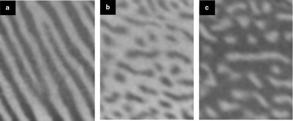
It is no coincidence that images of these magnetic domain patterns in figure 5 look similar to the compositional domain patterns in the Pb-Cu surface alloy system. The compositional and magnetic domain patterns are stabilized by long-range, dipolar repulsive forces competing with short-ranged ordering forces. The distance-dependence of magnetic dipolar interactions has the same form as the distance-dependence of the substrate-mediated strain fields causing repulsions in the surface alloy phase. In both systems, the competing forces drive the system toward minimum energy configurations consisting of ordered, equilibrium domain patterns. In fact, general models for two-phase two-dimensional systems with dipolar interactions describe explain exactly the type of behavior observed in these two rather different systems [11]. Such models predict stable striped domain patterns when the area fraction of the two domain types is near 1/2, while for relative domain area fractions in the region of 1/3 and 2/3 droplet- and inverse droplet-phases, respectively, should be observed.
Future directions
Remaining challenges in LEEM involve improving even further
the spatial resolution and pushing the time resolution from milliseconds to
nanoseconds or better. With its resolution of presently better than 50 Å, the
instrument built by Tromp et al., at IBM [12] approaches the limit imposed by
the accelerating field of the objective lens. The SMART project at the Bessy II
(Berlin Electron Storage Ring Society for Synchrotron Ratiation)
uses an electron mirror to correct for the aberrations of the objective lens;
researchers predict resolution resolution approaching
10 Å or better with such corrections [13].
A second approach, investigated at the
In addition
to the applications from examples provided in this article, a number of
exciting studies are filling the literature: temperature- or impurity-driven
faceting of initially uniform surfaces, structural phase formation and
separation during the growth of organic semiconductor thin films, and phase
separation during surface chemical reactions, among others. For a more extensive list, interested readers
may consult the reviews in references [12,15], the Web
site at http://www.leem-user.com, and the proceedings of the three
international workshops which have been held on LEEM and the related technique
of photoemission electron microscopy [16].
In PEEM, a UV or soft x-ray light source replaces the incident electron
beam, and photoelectrons provide chemical and surface potential contrast [17]. There are now working microscopes in several
laboratories in the
It is a pleasure to
acknowledge
References
[1] W.Telieps and
[2] K. Takayanagi, Y. Tanishiro, S. Takahashi and M. Takahashi, Surface Sci. 164, (1985).
[3] R. J. Phaneuf, Y. Hong, S. Horch and P. A. Bennett, Phys. Rev. Lett. 78, 4605 (1997).
[4] P. A. Bennett, M. Copel, D. Cahill, J. Falta and R. M. Tromp, Phys. Rev. Lett. 69, 1224 (1992).
[5] J. B. Hannon, F. J. Meyer zu Heringdorf, J. Tersoff and R. M. Tromp, Phys. Rev. Lett. 86, 4871 (2001).
[6] N. C. Bartelt, R. M. Tromp and E. D. Williams, Phys. Rev. Lett. 73, 1656 (1994); W. Theis, N. C. Bartelt, and R. M. Tromp, Phys. Rev. Lett. 75, 3328 (1995); R. M. Tromp and M. Mankos, Phys. Rev. Lett. 81,1050 (1998).
[7] R. Plass, J. A. Last, N. C. Bartelt and G. L. Kellogg, Nature 412, 875 (2001).
[8] M.S. Altman, H. Pinkvös, J. Hurst, H. Poppa, G. Marx, and E. Bauer, Mater. Res. Soc. Symp. Proc. 232, 125 (1991)
[9] T. Duden, and
[10] H. Poppa, E.D. Tober, and A.K. Schmid, J. Appl. Phys. 91, 6932 (2002)
[11] Kwok-On Ng and David Vanderbilt, Phys. Rev. B52, 2177 (1995)
[12] R. M. Tromp, IBM J. Res. Develop. 44, 503 (2000).
[13] R. Wichtendahl, et al., Surf. Rev. Lett. 5,1249 (1998).
[14] G. Schönhensee and H. Spiecker, J. Vac Sci Technol. B, in press (2002).
[15] E. Bauer, Rep. Prog. Phys. 57, 895 (1994); E. Bauer, Surf. Rev. Lett. 5, 1275 (1998).
[16] The proceedings of the first three International LEEM/PEEM workshops have been published in: Surf. Rev. Lett., 5, no.6 (1998); Surface Sci. 480, no. 3 (2000); J. Vac. Sci. Technol. B 20, no. 6 (2002).
[17] S. Günther, B. Kaulich, L. Gregoratti and M. Kiskinova, Prog. Surf. Sci. 70, 187 (2002).
*Raymond Phaneuf is an Assistant
Professor in the Department of Materials and Nuclear Engineering at the
University of Maryland College Park National Center Lawrence Berkeley Berkeley , California
Tutorial: The Basic Principles of LEEM
How does an electron microscope work? Essentially, electrostatic or magnetic lenses focus an electron beam onto a sample to illuminate a certain field of view; the scattered electrons are the collected and refocused onto a phosphor screen to form an image. What distinguishes low-energy electron microscopes (LEEMs) from the crowd is the energy range of the illuminating electrons, which are reduced to between 1 and 100 eV-far less than the 100 000 eV typically used in the more common transmission electron microscopes (TEMs). The useful energy ranges for these two techniques differ by many orders of magnitude because they exploit different scattering angles. High-energy electrons, scatter through small angles, and the dominance of forward scattering allows electrons to penetrate thin samples for investigations of sample’s interior structures. In LEEM, a reflection-geometry is more suitable: Low energy electrons scatter through large angles, making backscattering intensities high. At normal-incidence, it is common for crystalline samples illuminated with electrons of a few eV energy to elastically reflect a substantial fraction of the electrons (sometimes nearly all of them!) straight back toward the electron source. That reflectance explains why low energy electron beams are such attractive candidates for making high-brightness images of surface structures.
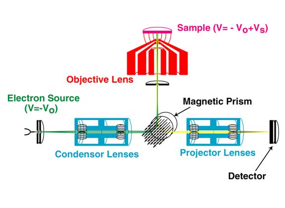
Nevertheless, the backscattering geometry is a challenge for LEEM instrumentation design. The column containing the illumination optics and the column containing the imaging optics both have to be arranged in front of the sample surface. In fact, for best imaging conditions it is often desirable that the illuminating beam and the reflected image beam share a common optical axis in the direction normal to the sample surface. Therefore a beam-separation element is needed somewhere along that optical axis. In most LEEM’s, a magnetic sector (B in the figure) is used to bend the illuminating beam onto the axis normal to the sample surface. Electrons reflected from the sample travel back on the same axis to reach again the prism, where they deflect further, into an imaging column that is separate from the illumination column.
The practicality of building a microscope that operates at energies of a few eV has also been a challenge. Electron optical lenses focus electrons poorly at energies much less than 10 keV due to the variation in focal length with energy and the energy spread associated with practical electron sources. The blurring that results is proportional to the ratio of the energy spread to the average energy and thus increases as the reciprocal of the energy. Ernst Bauer solved that problem by combining conventional, moderately high-energy electron optics (focusing the beam, at eV0) with a special objective lens that decelerates the incident electrons in the last few millimeters before they reach the sample, and reaccelerates the reflected electrons before they are refocused. Thus the sample, which is reverse biased at –V0+VS, sits in a strong electrostatic field and becomes an integral part of the imaging optics. Bauer predicted that the imaging properties of this electrostatic field should limit the resolution achievable by the objective lens, and consequently, of the entire microscope. Numerical calculations using typical values of sample-lens separations, field strengths, and energy spreads yielded a predicted optimum resolution in conventional LEEM instruments of approximately 35 Å.
The sensitivity of low-energy electrons to near-surface atomic layers explains their appeal and governs image contrast in LEEM. High-energy electrons used, say, in TEM penetrate deeply into the electron shells of atoms, so that nuclear charge is one of the most important factors governing contrast. In LEEM, the low-energy electrons never even get close to atomic nuclei; rather the detailed structure of the outer electron shells of atoms near the sample surface determines image contrast. Chemical bonds between atoms can be regarded as an example of electronic structure in outer electron shells; indeed, LEEM image contrast depends very sensitively on subtle differences of the chemical composition or crystal structure of topmost atomic layers. An image’s bright and dark areas, for ordered surfaces, come in part from satisfying or not satisfying the Bragg condition, leading to large variations in intensity with incident energy; for disordered structures the variations, and maximum intensity are considerably smaller. Defects such as atomic height steps or dislocations, as well as phenomena such as quantum well states in thin films can often be imaged with very good contrast. Or, if a spin-polarized (SP) electron beam is used for illumination, (from so-called SPLEEM instruments) surface magnetization directions show contrast.