GCA DSW 4800 Baseline Correction
Introduction
Baseline correction is an adjustment to the nominal offset of the X
and Y stages from the optical axis. It is also used to determine the angle
between the stage X-axis motions and the alignment microscope objectives
(microscope theta error).
Equipment and Materials
-
Three inch silicon wafer, coated with HMDS and positive photoresist, pre-baked
as required.
-
Baseline Correction Reticle.
-
Photoresist developer, glassware.
-
 Baseline
Correction Data Sheet.
Baseline
Correction Data Sheet.
Test Set-up
Use a copy of the BASLIN file located in the $!!$DX0 directory.
Test Procedure
Note: Using a previously exposed wafer to do the theta correction steps
(marked * below) first may avoid some x-y error, which may result
in fewer procedure repetitions necessary to bring the correction to the
desired tolerance.
-
Load and align baseline correction reticle.
-
Load prepared wafer.
-
EXEC BASLIN PASS 1, using full exposure time.
-
Expose the photoresist.
-
Do not post-bake photoresist.
-
Develop wafer for one-half of the usual time.
-
Reload wafer into stepper and EXEC BASLIN PASS 2, using full exposure time.
-
*Align wafer in X-Y-Theta BUT DO NOT YET EXPOSE.
-
*Press Control and T keys at the same time. Push the X, Y joystick to the
left. This will "jog" the wafer so that the right key will now appear in
the left side of the alignment monitor (i.e. stage moves so that the right
key is now under the left microscope objective). If there is no theta error,
the key will be aligned in Y (not necessarily in X though). If the key
is not well aligned in Y, adjust the theta micrometer located on the left-rear
side of the lens column to bring the key into alignment.
-
*Push the X, Y joystick to the right to bring both keys back into view
on the alignment monitor. The keys should still be well aligned; if not,
press the Control and E keys to disable the jog mode and realign keys.
Repeat as necessary.
-
Expose wafer for full exposure time.
-
Develop wafer using full development time.
-
Do not post-bake the photoresist.
-
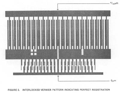
Locate and read the right-side X-axis vernier Record the readings on the
Baseline Correction Data Sheet.
-
Locate and read the right-side Y-axis vernier. Record the readings on the
Baseline Correction Data Sheet.
-
Locate and read the left-side Y-axis vernier. Record the readings on the
Baseline Correction Data Sheet.
-
Using the MODE command, read and record the current Baseline Correction
values.
-
Using the vernier readings from the right-side vernier, calculate and record
the new Baseline Correction values as follows:
New X value = Old X value - (right-side X vernier(µm)/1000)
New Y value = Old Y value - (right-side Y vernier(µm)/1000)
(Algebraic subtraction: [(-1) - (-1) = 0] and [(-1) - (+1) = -2)
Enter the new Baseline Correction values into MODE.
Calculate and record the alignment microscope theta error as follows:
theta error = (Y vernier left-side) - (Y vernier right-side).
(Algebraic subtraction: [(-1) - (-1) = 0] and [(-1) - (+1) = -2)
If the theta error is more than +/- 0.1 micron, then the theta micrometer
needs further adjustment.
Perform another baseline correction to verify that the new baseline correction
values are correct.
| X & Y AXIS BASELINE CORRECTION |
Current
Correction
From MODE |
Less
- |
Vernier
(µm ÷ 1000) |
Equals
= |
New
Correction |
| X-Axis |
- |
X-Axis Right Die |
= |
X Correction |
| Y-Axis |
- |
Y-Axis Right Die |
= |
Y Correction |
| THETA ERROR |
Vernier
(µm) |
Less
- |
Vernier
(µm) |
Equals
= |
Theta Error |
| Y-Axis Left Die |
- |
Y-Axis Right Die |
= |
Theta Error |
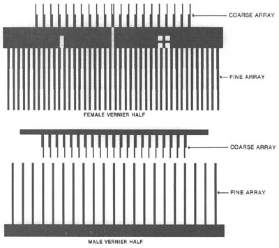
Vernier Reticle
The vernier reticle has X and Y axis arrays, each composed of a female
array and a male array, which in turn are each composed of a fine array
and a coarse array. The fine array (larger structures) measures -1 to +1
µm in 0.1 µm increments. The coarse array (smaller structures)
measures -10 to +10 µm in 1.0 µm increments. The fine and coarse
verniers are not cyclic, which is to say that either the fine array is
read or the coarse array is read, but not both. Therefore, a reading such
as 1.1 µm is impossible. If a reading of more than 1 µm is
made, it is necessary to make a baseline correction adjustment in MODE
for that reading to reduce the error to less than 1 µm, which will
bring the error into the range of the fine verniers. Then another baseline
correction procedure needs to be performed in order to reduce the error
in the sub-micron range.
File BASLIN in $!!$DX0 directory:
Metric Job Comment: Baseline Correction
Tolerance (1,2,*3,4,5,6): 1
Scale Corrections
X, PPM (-128<P<+128):
Y, PPM (-128<P<+128):
Orthogonality, PPM (-128<P<+128):
Wafer Diameter: 76.00000
<<ARRAY PARAMETERS>>
Step Size in X: 12.70000
*C-ount, S-pan or A-ll:
How Many Columns?: 6
Step Size in Y: 12.70000
*C-ount, S-pan or A-ll:
How Many Rows?: 6
Tranlate Origin
In X:
In Y:
Display? (Y/*N):
IF DISPLAY (Y) IS CHOSEN:

Pass #0 Array 24 Exposures Total Exposures=24
  1 2 3 4 5 6
1     X X
2   X X X X
3 X X X X X X
4 X X X X X X
5   X X X X
6     X X
Alignment Dice are Standard
R: 4
C: 6
R: 4
C: 1
|
Layout? (Y/*N):
IF LAYOUT? (Y) IS CHOSEN:

Array Has:              Centered:
6 Rows                  3,4
6 Cols                  3,4
1st Row, Col:
x = -31.75000
Y = -31.75000
|
Adjust? (Y/*N):
<<ALIGNMENT PARAMETERS>>
Standard Keys? (*Y/N):
Key Offset
In X: 0.27000
In Y: -0.52100
EPI Shift
In X:
In Y:
<<PASS>>
Name: 1
Comment: First Pass Baseline Correction
Exposure (Sec.): [Enter Appropriate Exposure Time]
Focus Setting: [Enter Appropriate Focus Setting]
Shift
In X:
In Y:
A-rray, P-lug or L-abel: P
Plugs:
R:
IF "V" IS ENTERED:
R: 4     +0.00000
C: 6     +0.00000
R: 4     +0.00000
C: 1     +0.00000
|
IF "D" IS ENTERED:
PASS 1   1 PLUG   2 EXPOSURES     TOTAL EXPOSURES=2
  1 2 3 4 5 6
1
2
3
4 X         X
5
6
ALIGNMENT DICE ARE STANDARD
R: 4
C: 6
R: 4
C: 1
|
<<END OF PASS SETUP>>
SAVE PASS? (*Y/N):
<<PASS>>
Name: 2
Comment: Second Pass Baseline Correction
Exposure (Sec.): [Enter Appropriate Exposure Time]
Focus Setting: [Enter Appropriate Focus Setting]
Shift
In X: 0.50000
In Y: 0.50000
A-rray, P-lug or L-abel: P
Plugs:
R:
IF "V" IS ENTERED:
[SAME PARAMETERS DISPLAYED AS FOR PASS 1]
|
IF "D" IS ENTERED:
[SAME AS PASS 1 WITH THE FOLLOWING EXCEPTION:]
PASS 2   2 PLUG   2 EXPOSURES     TOTAL EXPOSURES=2
|
<<END OF PASS SETUP>>
SAVE PASS? (*Y/N):
<<PASS>>
Name (<CR> to Exit Pass Setup):
Output Device Specification:
File Already Exists. Replace with New File? (*Y/N):
:
File MODE in $!!$DX0 directory:
Metric or English Units? (M/E): M
Scale Corrections
X, PPM (-128<P<+128):
Y, PPM (-128<P<+128):
Orthogonality, PPM (-128<P<+128): -8
Chuck Size (A,B,2,3,82,100,125): 3
Base Line Correction (MMS)
X: Current Value [Make Correction Here]
Y: Current Value [Make Correction Here]
Objective Spacing: 63.50000
Round Tube Compatibility (Y/*N):
Library User ID & Disk Desired? (Y/*N):
Use Auto Wafer Handler? (*Y/N):
Loading Correction
X: 80.00000
Y: -35.00000
Use Automatic Wafer Alignment? (Y/*N):
Use Programmable Focus Control? (*Y/N):
Set Focus in Mode? (Y/*N):
***HISTORY FILE PARAMETERS***
Log In, Log Out, Boots, Shutdowns, and Laser Origination? (Y/*N):
Wafer Transfer Times? (Y/*N):
System Fault Messages? (Y/*N):
EXEC Parameters? (*Y/N):
EXPO and AEXPO Parameters? (*Y/N):
Operator Comments? (Y/*N):
MODE Parameters? (Y/*N):
System Level Interaction? (Y/*N):
Wafer Batch Names? (Y/*N):
*****END OF HISTORY FILE PARAMETERS*****
Write Lock DX0? ((Y/*N):
Write Lock DX1? ((Y/*N):
Save Mode Data on Disk? (*Y/N):
: