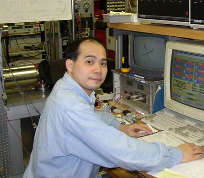

Born:Nov.10,1966,
Education: B.S. Electrophysics (1988), National Chaio-Tung Univ. Taiwan
Ph.D. Physics (1997),
Current Status : Assistant Research Scientist, Physics Dept., UMCP
Advisor: R. J. Phaneuf, Materials
Professional Interests: Structural evolution of semiconductor surfaces under eptiaxial growth or high temperature sublimation conditions;
Low energy electron microscopy; Electron optical simulations;
.
Current Projects :
- Development of the low energy electron microscope: Low energy electron microscopy (LEEM) is a powerful tool that allows real time imaging of the evolution of material surfaces under conditions such as high temperature annealing, and evaporative growth. We designed and built a low energy electron microscope at the Laboratory for Physical Sciences[1]. With our LEEM, we have characterized the mirror mode imaging of a lithographically patterned Si surface[2]. Through the construction and characterization of the microscope, we also developed a set of Fortran-based programs to numerically simulate the performance of individual electron optical elements. With this capability, we were able to check the performance of the magnetic prism against the simulation[3], which lead to a design of true stigmatic imaging magnetic prism[4]. We currently continue on fine tuning the performance of the microscope to improve the image resolution.
- Evolution of patterned semiconductor surfaces: As the device dimension of integrated circuits getting smaller down to nanometer scales, the relaxation of the artificially fabricated microscopic structures during the device processing procedures and the interaction between the surface defects, such as steps, and the impurities will have stronger impact on the performance of the devices. With lithographic tools, we pattern single crystal semiconductor surfaces with topographic structures or impurity features whose critical dimensions vary in a combinatorial manner. This allows us to characterize the size dependence of the evolution of the surface structures under device processing conditions such as epitaxial growth and high temperature annealing in ultra-high vacuum environment.
References
1. "Imaging Surface Dynamics in Real
Time with Low Energy Electron Diffraction" (Invited), Raymond J.
Phaneuf and
- “Focusing of low energy electrons by sub-micrometer patterned structures in low energy electron microscopy”, H.-C. Kan and R. J. Phaneuf, J. Vac. Sci. Technol. B 19,1158 (2001)
- H.-C. Kan, D. Auerbach, and R. J. Phaneuf, “A novel approach for investigating the astigmatism of a magnetic prism in low energy electron microscope”, Rev. Sci. Instru., in press, 2003.
- H.-C. Kan, T. Dürkop, and R. J. Phaneuf, “A Comparison of Stigmatically Focusing Magnetic Prisms of Square vs. Round Symmetries”, J. Vac. Sci. Technol. B 20,2519, (2002)
My Research is funded by the Laboratory for Physical
Sciences and a National Science Foundation Materials Science and
(LPS Webpage link) (MRSEC Webpage link)

